🚚 Free Worldwide Shipping on All Orders!Shop Now
$6.49
Original: $21.65
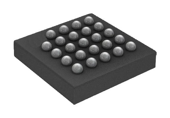
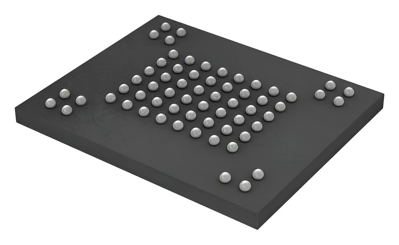
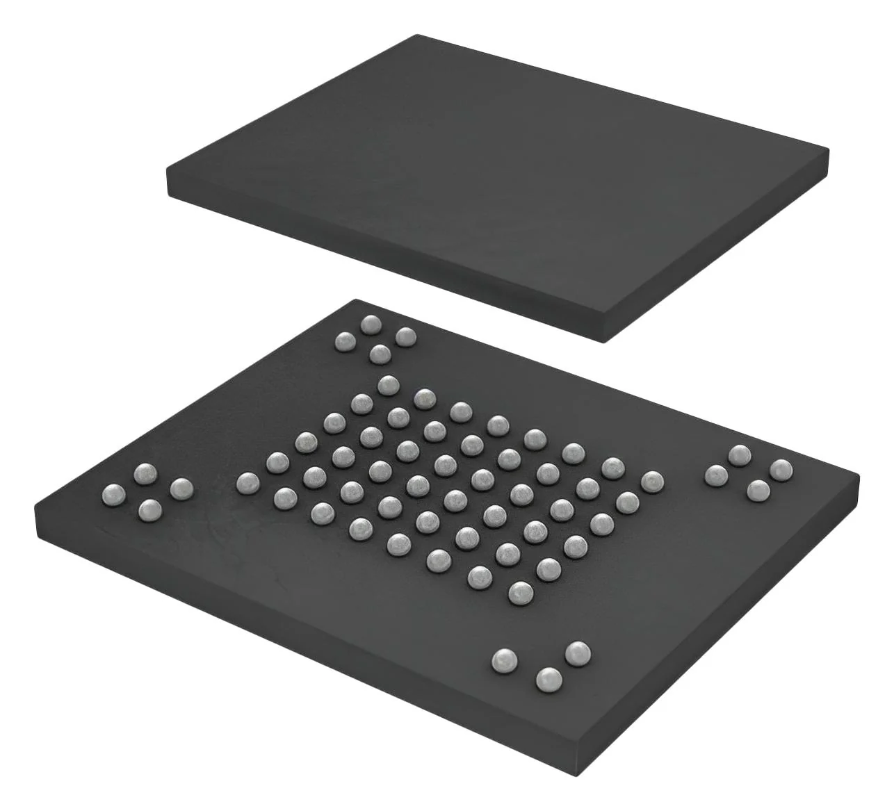
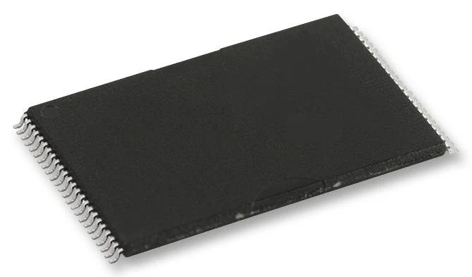
-70%MICRON MT29F4G16ABBDAH4-IT:D Flash Memory, SLC NAND, 4 Gbit, 256M x 16bit, Parallel, VFBGA, 63 Pins—
$21.65
$6.49The Story
MT29F4G16ABBDAH4-IT:D is a NAND flash device which includes an asynchronous data interface for high-performance I/O operations. This device uses a highly multiplexed 8-bit bus (I/Ox) to transfer commands, address, and data. There are five control signals used to implement the asynchronous data interface: CE#, CLE, ALE, WE#, and RE#. Additional signals control hardware write protection and monitor device status (R/B#). This hardware interface creates a low pin-count device with a standard pinout that remains the same from one density to another, enabling future upgrades to higher densities with no board redesign. A target is the unit of memory accessed by a chip enable signal. A target contains one or more NAND flash die. A NAND flash die is the minimum unit that can independently execute commands and report status. A NAND flash die, in the ONFI specification, is referred to as a logical unit (LUN).
- 4Gb density, 16-bit device width
- SLC level, 1.8V (1.7 to 1.95V) operating voltage
- Feature set D, Async interface
- Single-level cell (SLC) technology, command set: ONFI NAND flash protocol
- Program page cache mode, read page cache mode, one-time programmable (OTP) mode
- Operation completion, pass/fail condition, write-protect status
- Ready/Busy# (R/B#) signal provides a hardware method of detecting operation completion
- WP# signal: write protect entire device
- Industrial operating temperature range from -40°C to +85°C, package style is 63-ball VFBGA
Product details
| Flash Memory Type: SLC NAND |
| Memory Density: 4Gbit |
| Memory Configuration: 256M x 16bit |
| Interfaces: Parallel |
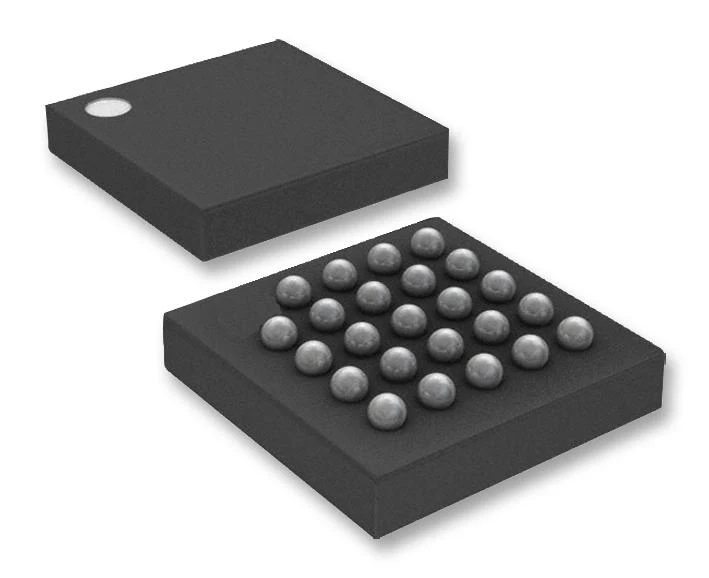
| IC Case / Package: VFBGA |
| No. of Pins: 63Pins |
| Clock Frequency Max: 50MHz |
| Access Time: 22ns |
| Supply Voltage Min: 1.7V |
| Supply Voltage Max: 1.95V |
| Supply Voltage Nom: 1.8V |
| IC Mounting: Surface Mount |
| Operating Temperature Min: -40°C |
| Operating Temperature Max: 85°C |
| Product Range: 1.7V-1.95V SLC NAND Flash Memories |
| MSL: MSL 3 - 168 hours |
Other details
| Brand | MICRON |
| Part Number | MT29F4G16ABBDAH4-IT:D |
| Quantity | Each |
| Technical Data Sheet EN |
All product and company names are trademarks™ or registered® trademarks of their respective holders. Use of them does not imply any affiliation with or endorsement by them.
Description
MT29F4G16ABBDAH4-IT:D is a NAND flash device which includes an asynchronous data interface for high-performance I/O operations. This device uses a highly multiplexed 8-bit bus (I/Ox) to transfer commands, address, and data. There are five control signals used to implement the asynchronous data interface: CE#, CLE, ALE, WE#, and RE#. Additional signals control hardware write protection and monitor device status (R/B#). This hardware interface creates a low pin-count device with a standard pinout that remains the same from one density to another, enabling future upgrades to higher densities with no board redesign. A target is the unit of memory accessed by a chip enable signal. A target contains one or more NAND flash die. A NAND flash die is the minimum unit that can independently execute commands and report status. A NAND flash die, in the ONFI specification, is referred to as a logical unit (LUN).
- 4Gb density, 16-bit device width
- SLC level, 1.8V (1.7 to 1.95V) operating voltage
- Feature set D, Async interface
- Single-level cell (SLC) technology, command set: ONFI NAND flash protocol
- Program page cache mode, read page cache mode, one-time programmable (OTP) mode
- Operation completion, pass/fail condition, write-protect status
- Ready/Busy# (R/B#) signal provides a hardware method of detecting operation completion
- WP# signal: write protect entire device
- Industrial operating temperature range from -40°C to +85°C, package style is 63-ball VFBGA
Product details
| Flash Memory Type: SLC NAND |
| Memory Density: 4Gbit |
| Memory Configuration: 256M x 16bit |
| Interfaces: Parallel |
| IC Case / Package: VFBGA |
| No. of Pins: 63Pins |
| Clock Frequency Max: 50MHz |
| Access Time: 22ns |
| Supply Voltage Min: 1.7V |
| Supply Voltage Max: 1.95V |
| Supply Voltage Nom: 1.8V |
| IC Mounting: Surface Mount |
| Operating Temperature Min: -40°C |
| Operating Temperature Max: 85°C |
| Product Range: 1.7V-1.95V SLC NAND Flash Memories |
| MSL: MSL 3 - 168 hours |
Other details
| Brand | MICRON |
| Part Number | MT29F4G16ABBDAH4-IT:D |
| Quantity | Each |
| Technical Data Sheet EN |
All product and company names are trademarks™ or registered® trademarks of their respective holders. Use of them does not imply any affiliation with or endorsement by them.