🚚 Free Worldwide Shipping on All Orders!Shop Now
$5.38
Original: $17.93
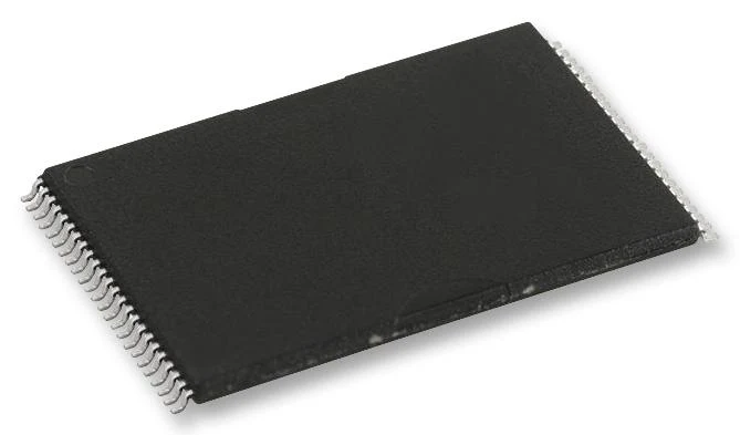
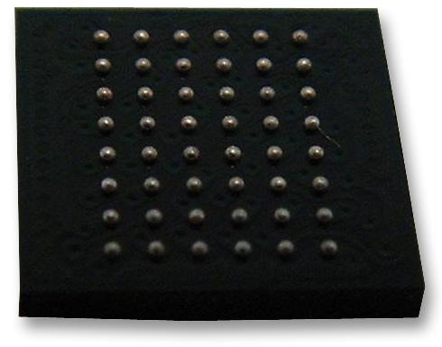
-70%Micron MT47H32M16NF-25E ITH Dram DDR2 512 Mbit 32M x 16bit 400 MHz Tfbga 84 Pins—
$17.93
$5.38The Story
MT47H32M16NF-25E IT:H is a DDR2 SDRAM. It uses a double data rate architecture to achieve high-speed operation. The double data rate architecture is essentially for 4n-prefetch architecture, with an interface designed to transfer two data words per clock cycle at the I/O balls. A single READ or WRITE operation for the DDR2 SDRAM consists of a single 4n-bitwide, two-clock-cycle data transfer at the internal DRAM core and four corresponding n-bit-wide, one-half-clock-cycle data transfers at the I/O balls. It has JEDEC-standard 1.8V I/O (SSTL_18-compatible) with differential data strobe (DQS, DQS#) option.
- Operating voltage range is 1.8V (VDD)
- 32Meg x 16 configuration, adjustable data-output drive strength
- Packaging style is 84-ball 8mm x 12.5mm FBGA
- Timing (cycle time) is 2.5ns at CL = 5 (DDR2-800)
- 4n-bit prefetch architecture
- Data rate is 800MT/s
- DLL to align DQ and DQS transitions with CK, programmable CAS latency (CL)
- Posted CAS additive latency (AL), WRITE latency = READ latency - 1�CK
- Adjustable data-output drive strength, 64ms, 8192-cycle refresh
- On-die termination (ODT), supports JEDEC clock jitter specification
Other details
| Brand | MICRON |
| Part Number | MT47H32M16NF-25E ITH |
| Quantity | Each |
| Technical Data Sheet EN |
All product and company names are trademarks™ or registered® trademarks of their respective holders. Use of them does not imply any affiliation with or endorsement by them. Image is for illustrative purposes only. Please refer to product description.
Description
MT47H32M16NF-25E IT:H is a DDR2 SDRAM. It uses a double data rate architecture to achieve high-speed operation. The double data rate architecture is essentially for 4n-prefetch architecture, with an interface designed to transfer two data words per clock cycle at the I/O balls. A single READ or WRITE operation for the DDR2 SDRAM consists of a single 4n-bitwide, two-clock-cycle data transfer at the internal DRAM core and four corresponding n-bit-wide, one-half-clock-cycle data transfers at the I/O balls. It has JEDEC-standard 1.8V I/O (SSTL_18-compatible) with differential data strobe (DQS, DQS#) option.
- Operating voltage range is 1.8V (VDD)
- 32Meg x 16 configuration, adjustable data-output drive strength
- Packaging style is 84-ball 8mm x 12.5mm FBGA
- Timing (cycle time) is 2.5ns at CL = 5 (DDR2-800)
- 4n-bit prefetch architecture
- Data rate is 800MT/s
- DLL to align DQ and DQS transitions with CK, programmable CAS latency (CL)
- Posted CAS additive latency (AL), WRITE latency = READ latency - 1�CK
- Adjustable data-output drive strength, 64ms, 8192-cycle refresh
- On-die termination (ODT), supports JEDEC clock jitter specification
Other details
| Brand | MICRON |
| Part Number | MT47H32M16NF-25E ITH |
| Quantity | Each |
| Technical Data Sheet EN |
All product and company names are trademarks™ or registered® trademarks of their respective holders. Use of them does not imply any affiliation with or endorsement by them. Image is for illustrative purposes only. Please refer to product description.