Original: $45.54
-70%$45.54
$13.66The Story
Product Overview
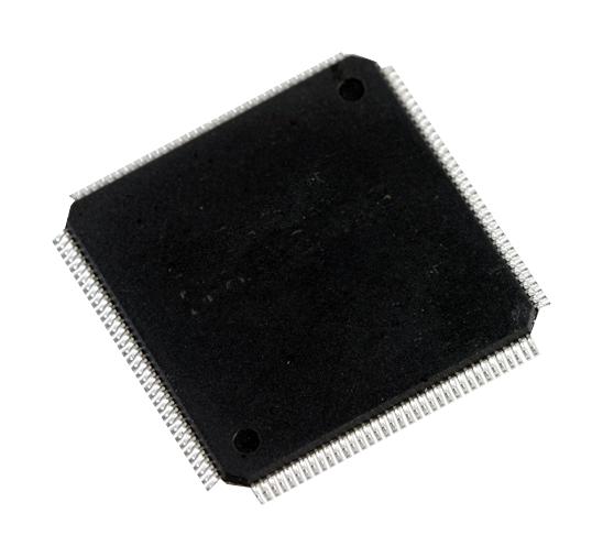
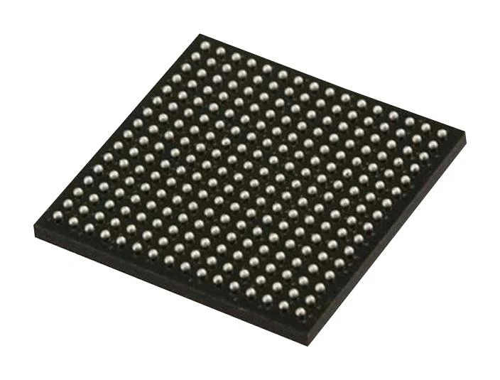
LCMXO2-4000HC-6FTG256I is an ultra low power, instant-on, non-volatile PLD FPGA. In addition to LUT-based, low-cost programmable logic, this device features embedded block RAM (EBR), distributed RAM, user flash memory (UFM), phase locked loops (PLLs), preengineered source synchronous I/O support, advanced configuration support including dual-boot capability and hardened versions of commonly used functions such as SPI controller, I²C controller and timer/counter. These features allow this device to be used in low cost, high volume consumer and system applications. The MachXO2 device is designed on a 65nm non-volatile low power process. This device architecture has several features such as programmable low swing differential I/O and the ability to turn off I/O banks, on-chip PLLs and oscillators dynamically. Applications include consumer electronics, compute and storage, wireless communications, industrial control systems, automotive system.
- 4320k logic capacity, standard device I/O count, high performance
- 2.5V/3.3V supply voltage, fastest speed
- Advanced 65nm low power process, as low as 22?W standby power
- Programmable low swing differential I/O
- Dedicated FIFO control logic, 100,000 write cycles
- Accessible through WISHBONE, SPI, I²C and JTAG interfaces
- Can be used as soft processor PROM or as flash memory
- DDR registers in I/O cells, dedicated gearing logic, 7:1 gearing for display I/O
- Generic DDR, DDRX2, DDRX4, dedicated DDR/DDR2/LPDDR memory with DQS support
- 256 lead ftBGA package, industrial operation junction temperature range from -40 to 100°C
Product details
Other details
| Brand | LATTICE SEMICONDUCTOR |
| Part Number | LCMXO2-4000HC-6FTG256I |
| Quantity | Each |
| Technical Data Sheet EN |
All product and company names are trademarks™ or registered® trademarks of their respective holders. Use of them does not imply any affiliation with or endorsement by them.
Description
Product Overview
LCMXO2-4000HC-6FTG256I is an ultra low power, instant-on, non-volatile PLD FPGA. In addition to LUT-based, low-cost programmable logic, this device features embedded block RAM (EBR), distributed RAM, user flash memory (UFM), phase locked loops (PLLs), preengineered source synchronous I/O support, advanced configuration support including dual-boot capability and hardened versions of commonly used functions such as SPI controller, I²C controller and timer/counter. These features allow this device to be used in low cost, high volume consumer and system applications. The MachXO2 device is designed on a 65nm non-volatile low power process. This device architecture has several features such as programmable low swing differential I/O and the ability to turn off I/O banks, on-chip PLLs and oscillators dynamically. Applications include consumer electronics, compute and storage, wireless communications, industrial control systems, automotive system.
- 4320k logic capacity, standard device I/O count, high performance
- 2.5V/3.3V supply voltage, fastest speed
- Advanced 65nm low power process, as low as 22?W standby power
- Programmable low swing differential I/O
- Dedicated FIFO control logic, 100,000 write cycles
- Accessible through WISHBONE, SPI, I²C and JTAG interfaces
- Can be used as soft processor PROM or as flash memory
- DDR registers in I/O cells, dedicated gearing logic, 7:1 gearing for display I/O
- Generic DDR, DDRX2, DDRX4, dedicated DDR/DDR2/LPDDR memory with DQS support
- 256 lead ftBGA package, industrial operation junction temperature range from -40 to 100°C
Product details
Other details
| Brand | LATTICE SEMICONDUCTOR |
| Part Number | LCMXO2-4000HC-6FTG256I |
| Quantity | Each |
| Technical Data Sheet EN |
All product and company names are trademarks™ or registered® trademarks of their respective holders. Use of them does not imply any affiliation with or endorsement by them.